- 您现在的位置:买卖IC网 > Sheet目录3872 > PIC18F4450T-I/ML (Microchip Technology)IC PIC MCU FLASH 8KX16 44QFN
2010 Microchip Technology Inc.
DS70141F-page 29
dsPIC30F3010/3011
3.1.1
DATA ACCESS FROM PROGRAM
MEMORY USING TABLE
INSTRUCTIONS
This architecture fetches 24-bit wide program memory.
Consequently,
instructions
are
always
aligned.
However, as the architecture is modified Harvard, data
can also be present in program space.
There are two methods by which program space can
be accessed: via special table instructions, or through
the remapping of a 16K word program space page into
the upper half of data space (see Section 3.1.2 “Data
The
TBLRDL
and
TBLWTL
instructions offer a direct method of reading or writing
the lsw of any address within program space, without
going through data space. The TBLRDH and TBLWTH
instructions are the only method whereby the upper 8
bits of a program space word can be accessed as data.
The PC is incremented by two for each successive
24-bit program word. This allows program memory
addresses to directly map to data space addresses.
Program memory can thus be regarded as two 16-bit
word-wide address spaces, residing side by side, each
with the same address range. TBLRDL and TBLWTL
access the space which contains the lsw, and TBLRDH
and TBLWTH access the space which contains the
MSB.
Figure 3-2 illustrates how the EA is created for table
operations and data space accesses (PSV = 1). Here,
P<23:0> refers to a program space word, whereas
D<15:0> refers to a data space word.
A set of table instructions are provided to move byte or
word-sized data to and from program space.
1.
TBLRDL:
Table Read Low
Word: Read the lsw of the program
address;
P<15:0> maps to D<15:0>.
Byte: Read one of the LSBs of the program
address;
P<7:0> maps to the destination byte when byte
select = 0;
P<15:8> maps to the destination byte when byte
select = 1.
2.
TBLWTL:
Table Write Low (refer to Section 6.0
“Flash Program Memory” for details on Flash
programming).
3.
TBLRDH:
Table Read High
Word: Read the msw of the program
address;
P<23:16> maps to D<7:0>; D<15:8> will always
be = 0.
Byte: Read one of the MSBs of the program
address;
P<23:16> maps to the destination byte when
byte select = 0;
The destination byte will always be = 0 when
byte select = 1.
4.
TBLWTH:
Table Write High (refer to Section 6.0
“Flash Program Memory” for details on Flash
programming).
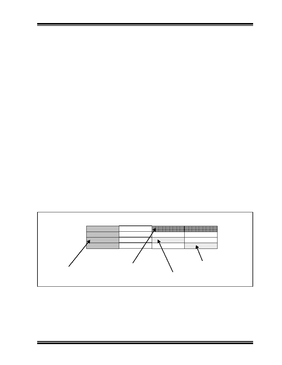
FIGURE 3-3:
PROGRAM DATA TABLE ACCESS (lsw)
0
8
16
PC Address
0x000000
0x000002
0x000004
0x000006
23
00000000
Program Memory
‘Phantom’ Byte
(Read as ‘0’).
TBLRDL.W
TBLRDL.B (Wn<0> = 1)
TBLRDL.B (Wn<0> = 0)
发布紧急采购,3分钟左右您将得到回复。
相关PDF资料
PIC18F4321T-I/ML
IC PIC MCU FLASH 4KX16 44QFN
PIC18F4221T-I/ML
IC PIC MCU FLASH 2KX16 44QFN
PIC18F2321T-I/ML
IC PIC MCU FLASH 4KX16 28QFN
PIC18F2221T-I/SO
IC PIC MCU FLASH 2KX16 28SOIC
PIC16LF1939-I/MV
IC MCU 8BIT 28KB FLASH 40-UQFN
PIC24F16KL402-I/SP
IC MCU 16BIT 16KB FLASH 28-SPDIP
PIC18F24J11-I/SS
IC PIC MCU FLASH 16K 2V 28-SSOP
PIC24F16KA101-I/SO
IC PIC MCU FLASH 16K 20-SOIC
相关代理商/技术参数
PIC18F4450T-I/PT
功能描述:8位微控制器 -MCU 16KB FL 768 RAM 34 I/O FS-USB 2.0 RoHS:否 制造商:Silicon Labs 核心:8051 处理器系列:C8051F39x 数据总线宽度:8 bit 最大时钟频率:50 MHz 程序存储器大小:16 KB 数据 RAM 大小:1 KB 片上 ADC:Yes 工作电源电压:1.8 V to 3.6 V 工作温度范围:- 40 C to + 105 C 封装 / 箱体:QFN-20 安装风格:SMD/SMT
PIC18F4455-BL
制造商:POWERLITE SYSTEMS 功能描述:PIC18F445 W/ BOOTLOADER FOR FLASHLAB 制造商:POWERLITE SYSTEMS 功能描述:PIC18F445 W/ BOOTLOADER, FOR FLASHLAB 制造商:POWERLITE SYSTEMS 功能描述:PIC18F445 W/ BOOTLOADER, FOR FLASHLAB; Silicon Manufacturer:Powerlite Systems; Core Architecture:PIC; Kit Contents:Board; Features:Bootloader Programming, RS232 Connector for Boot-Loading and Serial Comms ;RoHS Compliant: Yes
PIC18F4455-I/ML
功能描述:8位微控制器 -MCU 24kBF 2048RM FSUSB2 RoHS:否 制造商:Silicon Labs 核心:8051 处理器系列:C8051F39x 数据总线宽度:8 bit 最大时钟频率:50 MHz 程序存储器大小:16 KB 数据 RAM 大小:1 KB 片上 ADC:Yes 工作电源电压:1.8 V to 3.6 V 工作温度范围:- 40 C to + 105 C 封装 / 箱体:QFN-20 安装风格:SMD/SMT
PIC18F4455-I/P
功能描述:8位微控制器 -MCU 24kBF 2048RM FSUSB2 RoHS:否 制造商:Silicon Labs 核心:8051 处理器系列:C8051F39x 数据总线宽度:8 bit 最大时钟频率:50 MHz 程序存储器大小:16 KB 数据 RAM 大小:1 KB 片上 ADC:Yes 工作电源电压:1.8 V to 3.6 V 工作温度范围:- 40 C to + 105 C 封装 / 箱体:QFN-20 安装风格:SMD/SMT
PIC18F4455-I/PT
功能描述:8位微控制器 -MCU 24kBF 2048RM FSUSB2 RoHS:否 制造商:Silicon Labs 核心:8051 处理器系列:C8051F39x 数据总线宽度:8 bit 最大时钟频率:50 MHz 程序存储器大小:16 KB 数据 RAM 大小:1 KB 片上 ADC:Yes 工作电源电压:1.8 V to 3.6 V 工作温度范围:- 40 C to + 105 C 封装 / 箱体:QFN-20 安装风格:SMD/SMT
PIC18F4455T-I/ML
功能描述:8位微控制器 -MCU 24kBF 2048RM FSUSB2 RoHS:否 制造商:Silicon Labs 核心:8051 处理器系列:C8051F39x 数据总线宽度:8 bit 最大时钟频率:50 MHz 程序存储器大小:16 KB 数据 RAM 大小:1 KB 片上 ADC:Yes 工作电源电压:1.8 V to 3.6 V 工作温度范围:- 40 C to + 105 C 封装 / 箱体:QFN-20 安装风格:SMD/SMT
PIC18F4455T-I/PT
功能描述:8位微控制器 -MCU 24kBF 2048RM FSUSB2 RoHS:否 制造商:Silicon Labs 核心:8051 处理器系列:C8051F39x 数据总线宽度:8 bit 最大时钟频率:50 MHz 程序存储器大小:16 KB 数据 RAM 大小:1 KB 片上 ADC:Yes 工作电源电压:1.8 V to 3.6 V 工作温度范围:- 40 C to + 105 C 封装 / 箱体:QFN-20 安装风格:SMD/SMT
PIC18F4458-I/ML
功能描述:8位微控制器 -MCU 24KB Flash 2KB RAM RoHS:否 制造商:Silicon Labs 核心:8051 处理器系列:C8051F39x 数据总线宽度:8 bit 最大时钟频率:50 MHz 程序存储器大小:16 KB 数据 RAM 大小:1 KB 片上 ADC:Yes 工作电源电压:1.8 V to 3.6 V 工作温度范围:- 40 C to + 105 C 封装 / 箱体:QFN-20 安装风格:SMD/SMT